Explore Products for Electroless Copper
Have a question? Let us help you.
We are here to help you. Please feel free to contact us with questions, comments or feedback.
High-reliability Electroless Copper Plating Solutions for demanding Printed Circuit Board (PCB) applications, delivering optimal performance for multilayer boards.
Our M-Copper and Via Dep Electroless Copper Plating solutions and processes deliver unparalleled reliability, superior adhesion, and stress-free copper deposition for demanding Printed Circuit Board (PCB) applications, backed by global support and industry-leading technologies.
We are here to help you. Please feel free to contact us with questions, comments or feedback.
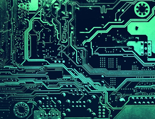
Electroless copper plating is a primary metallization process used in PCB manufacturing to create a conductive copper layer on non-conductive materials before electroplating. The process conditions the surface, applies a catalytic activation layer and deposits a uniform copper coating that enables reliable electrical connections. Electroless copper solutions provide excellent coverage for through-holes, microvias and complex PCB structures, supporting high-density interconnect (HDI), multilayer and flexible circuit applications. This technology helps manufacturers achieve consistent plating quality, improved reliability and efficient production for advanced printed circuit board fabrication.
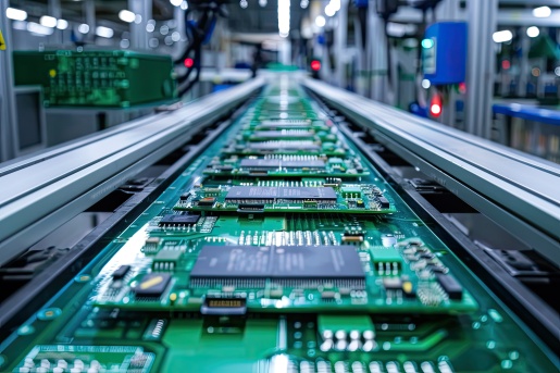
Electroless copper plating is used in advanced PCB manufacturing applications that require reliable, uniform copper deposition and excellent coverage. Common applications include Printed Circuit Boards (PCBs), flexible circuits, high-density interconnect (HDI) boards, microvias and complex multilayer substrates. It is especially valuable for challenging materials such as polyimides and high-frequency laminates where consistent adhesion and conductivity are critical. Electroless copper solutions enable precise through-hole metallization, support miniaturized designs and help manufacturers achieve high reliability, improved process efficiency and consistent performance in next-generation electronic devices.
Electroless copper plating improves PCB performance by creating a uniform, high-quality copper layer with excellent adhesion and coverage across complex board structures. This reliable primary metallization process enhances electrical conductivity, reduces signal loss and supports precise fabrication of fine-line circuits, microvias and high-density interconnect (HDI) designs. By enabling consistent through-hole metallization and dependable copper deposition, electroless copper solutions help PCB manufacturers improve production yields, assembly reliability and long-term performance in advanced electronic applications.
Key features of electroless copper plating include uniform copper deposition, excellent adhesion, low-stress copper layers and reliable coverage on complex, non-conductive substrate materials. This advanced primary metallization process enables precise plating of fine lines, microvias and intricate circuit designs required for high-density interconnect (HDI) and Modified Semi-Additive Process (mSAP) applications. Electroless copper solutions improve manufacturing consistency, support advanced PCB designs and deliver reliable electrical performance, making them ideal for high-performance electronics requiring superior plating quality, process control and long-term reliability.
Choosing the right electroless copper plating process depends on substrate materials, board design requirements, copper thickness, application performance needs and manufacturing goals. PCB manufacturers should evaluate solutions that provide uniform copper deposition, strong adhesion, reliable through-hole coverage and compatibility with advanced designs such as HDI, microvias and mSAP applications. Selecting the right electroless copper chemistry helps optimize process efficiency, improve production yields and deliver long-term reliability for high-performance printed circuit boards. Partnering with an experienced supplier ensures the process is matched to specific fabrication requirements.
Integrated Solutions
Our integrated PCB metallization portfolio combines electroless copper, direct metallization and advanced final finishes to deliver consistent, high-quality plating across diverse board materials. Designed for reliable PCB manufacturing, these solutions optimize copper deposition, process efficiency and production yields while supporting sustainable fabrication through improved resource utilization, reduced waste and advanced chemistry management.
Sustainability
Our precious metal-free primary metallization solutions support sustainable Printed Circuit Board (PCB) manufacturing by reducing resource consumption, minimizing process waste and improving production efficiency. Designed for advanced electroless copper applications, these technologies help manufacturers lower environmental impact while delivering reliable copper deposition, consistent plating performance and cost-effective solutions for high-quality PCB fabrication.
Reliability
Our direct and electroless copper primary metallization solutions deliver exceptional reliability for high-speed, multilayer and advanced Printed Circuit Boards (PCBs). Engineered for uniform copper deposition, strong adhesion and consistent through-hole coverage, these technologies help manufacturers achieve higher yields, improved signal integrity and long-term performance for demanding PCB fabrication applications.
Unlock high performance and increased board capacity with our conductive polymer-based direct metallization system.
Learn More
Achieve sustainability, cost savings, and reliability with our conductive hole-making processes that outperform traditional methods.
Learn More