Compugraphics
Semiconductor Photomasks for Wafer Fabrication and Prototyping
We provide high quality semiconductor photomasks and reticle solutions for wafer fabrication and prototyping to our customers around the globe.
Why Compugraphics?
At Compugraphics, We provide high quality semiconductor photomasks and reticle solutions for wafer fabrication and prototyping to our customers around the globe. We have gained a solid reputation for technical and service excellence through our responsiveness and meeting our customers' requirements for over 50 years.
Servicing our customers and adding value to their operations is at the heart of all we do. All of our customers are important to us and we want them to feel truly valued, whether they are in the start-up phase or are long-established clients. We share our knowledge and experience and always aim to understand the dynamics of their business, aligning their needs and our services accordingly.
By building quality into every stage of our processes, we create reliable products within the fast cycle times our customers require. In turn, this enables our customers to achieve the best possible manufacturing yield and lower their cost of ownership by delivering on time products to their end customer.
1X Master Photomasks
Ranging from 3”x 3” to 9”x 9” in a variety of substrate types, thickness and resist coatings for contact and projection aligners.
1X Masters are used in both mature and emerging applications by using mask aligner or scanner technology. The photomask contains the full image or array of the final wafer and then exposed in either a single exposure or scan. Please contact us for any non-standard requirements.
Contact Us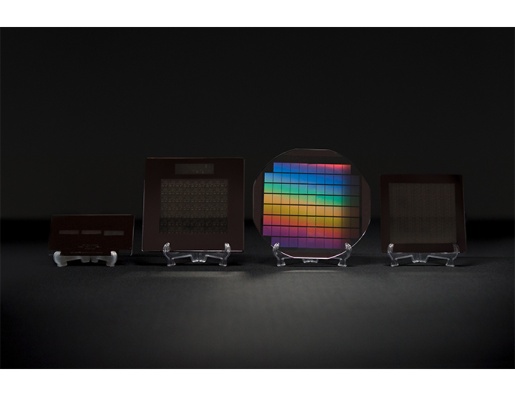
Reticles
Reduction reticles (1.8X, 2X, 2.5X, 4X, 5X, 10X) for various stepper types (e.g. ASML, Nikon, Canon) and 1X Ultratech reticles.
We produce both reduction reticles (1.8X, 2X, 2.5X, 4X, 5X, 10X) for a range of stepper types including Nikon, Canon, and ASML in addition to 1X Ultratech. Reticles can be ordered either with or without a pellicle. We also offer a pellicle replacement and recertification service.
Contact Us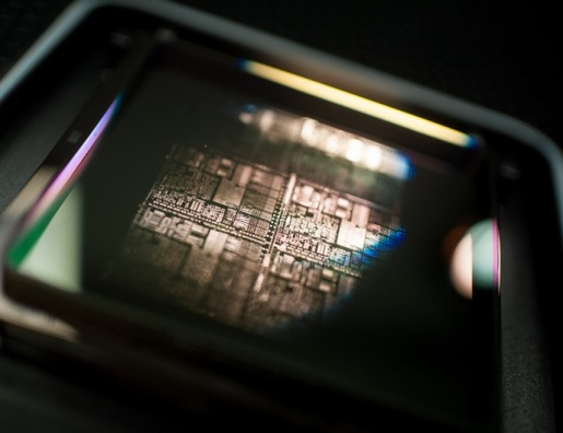
Large Area Masks
A variety of substrate types available (QZ, SL, Borofloat) and mask sizes up to 18”x 18”.
Contact Us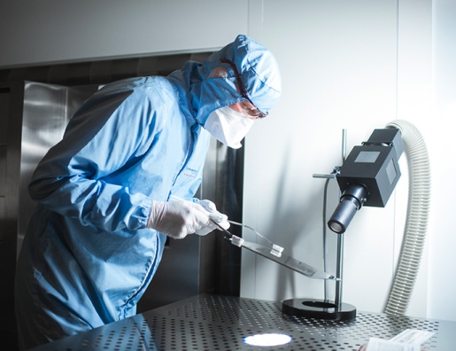
Direct Write Wafers
We can pattern your designs directly onto your supplied wafers. Ideal for prototyping, smaller runs and fast design requirements.
Direct Write enables patterning a design directly to wafer and eliminating the mask aligner and photomask process. We present your design file to our tool to write the pattern onto the resist covered substrate. This process ultimately delivers faster access to the final product.
Contact Us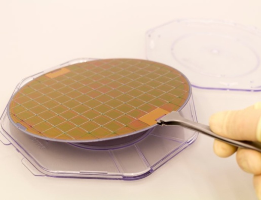
Copy Masks
Copy Masks, ranging from 3”x 3” to 7”x 7” on both soda lime and quartz substrate, for contact and close-proximity lithography.
If a master mask is used, then the cost of the replacement mask or duplicate would be the same as making a new mask. However, if the dimensions are large enough (>2μm) and the specifications for resolution, registration, and defectivity are less critical, then a copy of the mask can be made using a contact print process. This is less costly than making a new master mask.
Contact Us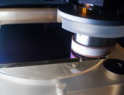
Grayscale Masks
Our Grayscale Mask Technology allows you to sculpt 3D structures in photoresist.
Contact Us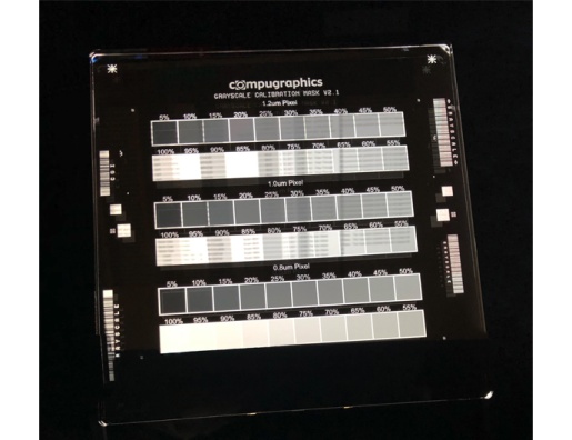
Support Services
Our Support Services
Our services and systems are developed with the aim of ensuring our customers’ operations can rely on our support from the design phase to delivery and mask use. From our focused, knowledgeable support team, to flexible online order systems, we are there when you need us.
Pellicle Replacement
Fast-turn support for pellicle replacement and mask recertification to minimize disruption to your operations and scheduling.
We offer this service to remove an existing pellicle on a photomask/reticle that is damaged or in any way compromised (handling, environmental trauma, age/deterioration, usage, etc.). The reticle is cleaned and the new required pellicle part added.
The repaired mask is inspected to ensure that the image quality has been maintained and returned to the customer to resume use with minimal loss of valuable production time.
We understand production lines are often down because of a single damaged pellicle, so we prioritize quick turns to minimize critical delays.
Contact UsMPT Coating
Our MPT coating extends the life of the photomask and improves throughput by increasing the number of exposures between mask cleanings.
MPT is a cost-effective way to reduce cycle time and improve wafer-process yield. While the thin, optically transparent coating reduces sticking to your mask during contact and proximity printing, the fluoropolymer reduces the number of mask cleanings, extending the life of the mask and improving throughput by increasing the number of exposures between mask cleanings. MPT is also chemical resistant with no effect on resolution.
Contact UsPhotomask Cleaning
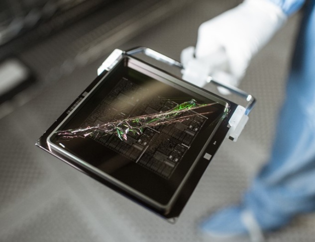
We offer after sales support of photomasks in use to remove contamination and prolong their lifetime. We service quick-turn requirements to minimize critical delays or line stop in fab.
Maintaining mask quality in usage is a challenge, and while photomasks are robust, they are not indestructible. The lithography processes used by our customers, regardless of sector, demand that the mask has a level of pattern integrity that enables devices to be manufactured without any imperfections, which may affect performance.
Our cleaning processes combine both chemical and physical methods. A mixture of sulphuric acid and hydrogen peroxide is used to remove photoresist and organic contaminants.
We prioritize quick turns to minimize critical delays or line-stop in fab.
Contact Us
Online Ordering and Reporting
Easy-to-use online Request for Quote Form, Mask Order Form, and Customer Portal for tracking live order status and shipments.
Our Customer Support, Engineering, and Commercial Teams are here to support and guide customers through mask definition and planning for their projects, regardless of the size of their operations.
We also understand the importance of providing 24/7 access to robust, easy-to-use online systems to allow you to place orders and check where your orders are in production or transit. Our customers enjoy the ability to access this information in real time no matter which time zone they are in.
Compugraphics also offers secure archiving of customer data to allow reordering of duplicate masks or to place an order for a remake if a mask is damaged in fab. Extended time periods for archiving can be agreed.
Contact UsData Prep Support
Conversions of supplied data to "ready-to-write", data verification checks, online remote data view, and approvals.
We provide solutions where you may lack in-house, including resources for data conversions, setup of supplied data to “write-ready” mask data formats, and/or creation of new data from your supplied instructions.
If you intend to supply DXF, please contact us and we can provide guidance to help save time, money, and possible conversion errors.
We can also provide all necessary guidelines for mask layout including fracture windows, grid size, frame generation, etc.
Contact UsPhotomasks - The Basics
Discover more on the basics of what a photomask is and how it is used. We offer expert support to help you clearly define your photomask needs.
A photomask is a quartz or glass substrate, coated with an opaque film into which is etched the design of the device being manufactured.
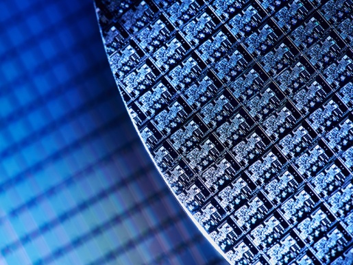
The photomask plays a critical role in the microlithography process used by our customers for the manufacture of integrated circuits (ICs), photonic devices, and micro-electro-mechanical systems (MEMS). A photomask consists of a fused silica (QZ) or glass (SL) substrate coated with an opaque film, into which an accurate replication of the device designer’s pattern is etched. In addition to a high degree of pattern fidelity, the photomask also has to meet our customers’ expectations for line width, critical dimension (CD) control, pattern placement (registration), and defectivity control. The terms "masters", "sub-masters", and "copy masks" are usually used to refer to 1X photomasks, while the term "reticles" refers to 1.8X, 2X, 2.5X, 4X, 5X, and 10X stepper or scanner photomasks. A functioning device can require between 5 to 40+ individual photomasks, one mask for each step used in the fabrication process.
Contact Us