Browse Applications by Category

Aerospace Applications
The aerospace industry uses various solders, adhesives, and materials as well as hermetically sealed packages in many systems within aerospace design.
Hermetic Packaging
Hermetic packaging seals in an airtight environment, employing inorganic substrates such as various metals, ceramics or glass to isolate critical microelectronics from the surrounding environment.

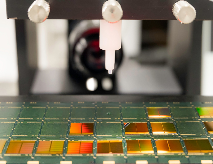
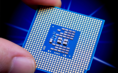
Heterogeneous Integration (2.5/3D)
Heterogenous integration through 2.5/3D packaging involves interconnecting various active or passive components to achieve system level functionality in a single package.
Laminate Packaging
Laminate packaging adopts a Ball-Grid-Array (BGA) design, attaching the die on a plastic or tape laminated substrate with the electrical connections on the bottom of the package.
Leadframe Packaging
Leadframe packaging contains a semiconductor die/chip on metal pads encapsulated in molding compound with metal leads around the perimeters of the package.

Medical Device
The implantable medical industry uses hermetic packages within the human body to protect and ensure electronic functionality in pacemakers, defibrillators, neuromodulators, and hearing devices.
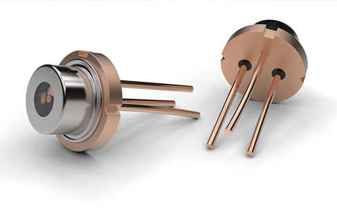
Optoelectronics Packaging
The optical networking industry largely focuses on electronic systems and devices that source, detect and control light.

Power Discrete
Power discrete is a single semiconductor device used as a switch or rectifier in power electronics.

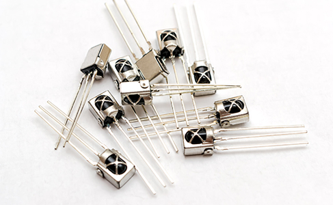
Sensors
Sensors boast low cost, low power, durability, and reliability while being “always on”. They are impervious to dirt, dust and the environment, employing various photonics and light technologies. Sensors implement Bluetooth technology, faster communication speeds, data communication and channels.
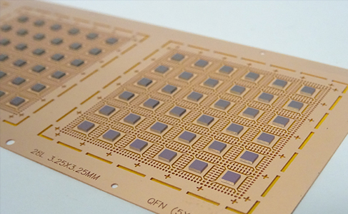
System in Package (SiP)
System in Package (SiP) is a combination of active electronic components with various functions and passive components, assembled in a single package to provide an integrated system level function.
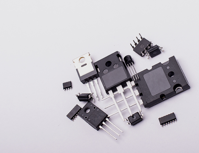
Power Semiconductor
Power semiconductor is a semiconductor device used as a switch or rectifier in power electronics.