MICROFAB® SC-40 PLUS
Next-generation high-speed copper plating process delivers high-purity deposits with cutting-edge uniformity.
Contact UsProduct Overview
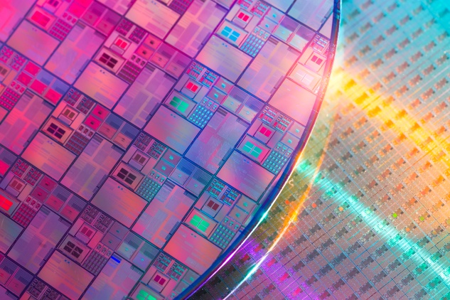
MICROFAB SC-40 PLUS, a next-generation acid copper plating process, represents a leap forward in semiconductor manufacturing. It provides fabricators with a transformative solution that combines precision, efficiency, and ease of use. With high-speed plating capabilities of up to 2.5 µm/min, MICROFAB SC-40 PLUS delivers a high purity deposit with exceptional within-wafer, within-die and within-feature uniformity.
Product Features
Innovative Copper Pillar Plating for Next-Generation Packages
MICROFAB SC-40 PLUS is designed to meet the semiconductor industry’s need for enhanced reliability and performance of advanced packages.
High Purity Deposit with Cutting-Edge Uniformity
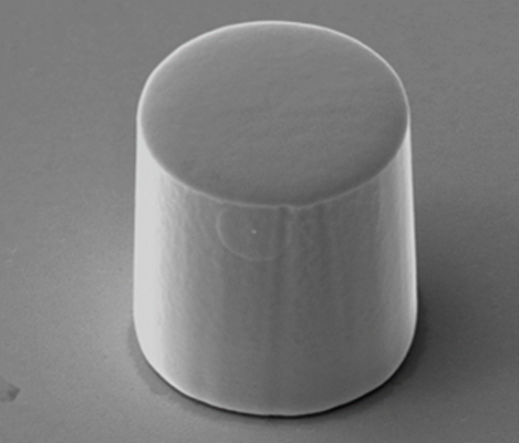
The process is capable of high-speed plating up to 2.5 µm/min, enabling a high purity deposit with exceptional uniformity and a flat bump profile.
Versatile Chemistry Enables Ease of Use
Versatile chemistry for different Aspect Ratio (AR) Pillar and L/S of Redistribution Layer (RDL). The process is compatible with and without a nickel barrier process, ensuring Kirkendall Void (KV)-free stacks.
Next-Generation Packaging Solutions
MICROFAB SC-40 PLUS is part of the next generation of our SC products and processes, a range with over 10 years in the market. It represents a leap forward in semiconductor manufacturing, providing fabricators with a transformative solution that combines precision, efficiency, and ease of use.
Reliability Excellence
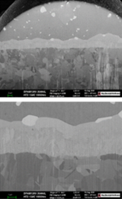
MICROFAB SC-40 PLUS is a highly pure system designed to eliminate interfacial voids across a range of applications, including pillar, Under-Bump Metallization (UBM), and Line/Space (L/S) RDL. During harsh Joint Electron Device Engineering Council (JEDEC) reliability tests, the copper/solder interface exhibits no voids. The excellent reliability of MICROFAB SC-40 PLUS is maintained even as the bath ages.
Featured Applications
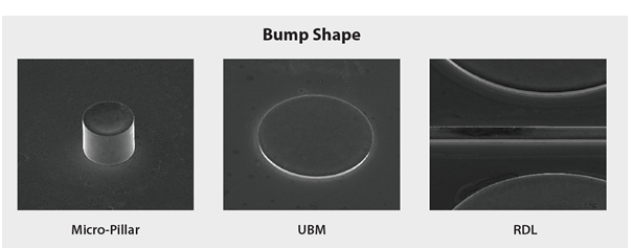
Bump, Pillar and RDL
MICROFAB SC-40 PLUS is suitable for bump, pillar, and RDL metallization and is compatible with or without a nickel barrier, as well as various solders such as tin silver and pure tin.