M-Speed HF
Low-etch oxide alternative coating provides low surface profiles and reliable adhesion for high-frequency applications.
DiscoverUnleash the potential of your high-frequency, next-generation designs with our advanced innerlayer adhesion promotion technology treatment systems.
Our copper adhesion promotion technologies ensure enhanced reliability, low signal attenuation, and precise process control, meeting the demands of today’s high-data-rate and high-frequency operating systems for printed circuit formation.

Our copper surface treatments optimize innerlayer adhesion, ensuring high reliability and durability across various materials in high-performance applications.
Our low-etch systems minimize surface roughness, reducing signal transmission loss and improving performance in high-frequency and high-data-rate applications.
Our controlled etch products enable the creation of fine features in Semi-Additive Process (SAP) and Modified Semi-Additive Process (mSAP) applications, preserving trace geometry and current capacity for high-density Printed Circuit Board (PCBs) and Integrated Circuit (IC) substrates.
Our leadframe adhesion promotion products deliver MSL-1 reliability, ensuring robust performance for evolving automotive electronics and Advanced Driver Assistance Systems (ADAS).
Our leadframe portfolio includes solutions for roughening, enhanced sidewall solderability, and more. We support the entire Quad-Flat No-Leads (QFN) package building process.
Signal loss in high-frequency PCB and IC substrate applications can be mitigated through both material selection and surface engineering. In addition to optimized dielectric base materials, using advanced adhesion promotion technologies that create minimal copper surface roughness helps reduce signal attenuation and improve signal integrity. Smoother copper interfaces lower conductor loss, enabling better high-speed signal transmission for HDI and high-frequency designs. These circuit formation solutions support improved impedance control, reduced insertion loss, and enhanced reliability in demanding applications such as 5G, data centers, automotive radar, and advanced computing. The result is higher performance, lower defects, and more stable high-speed electronic operation.
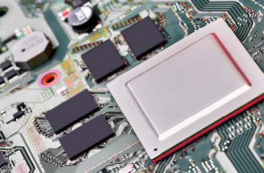
Adhesion plays a critical role in printed circuit board (PCB) manufacturing by ensuring strong, thermally robust bonding between copper layers and laminate materials. This adhesion is essential for maintaining structural integrity, preventing delamination, and ensuring long-term electrical and mechanical reliability under thermal cycling and high-stress operating conditions. Advanced adhesion promotion technologies also improve copper interface quality, support fine-line circuitry, and enhance signal integrity in high-density interconnect (HDI) and IC substrate applications. By strengthening layer-to-layer bonding, these solutions improve manufacturing yield, reduce defects, and enable reliable performance in demanding electronics such as automotive, data center, industrial, and high-frequency devices.
Leadframe solutions enhance reliability in QFN (Quad Flat No-Lead) packaging by optimizing key surface preparation and metallization processes that ensure strong, consistent electrical and mechanical performance. These integrated circuit formation technologies include roughening for improved adhesion, burr removal for structural integrity, anti-bleed control, and enhanced sidewall solderability for secure interconnects. Together, these steps improve conductivity, reduce defect risks, and strengthen package robustness under thermal cycling and mechanical stress. The result is higher assembly yield, improved signal integrity, and long-term reliability for advanced semiconductor packaging used in automotive, industrial, consumer, and high-performance electronic applications.
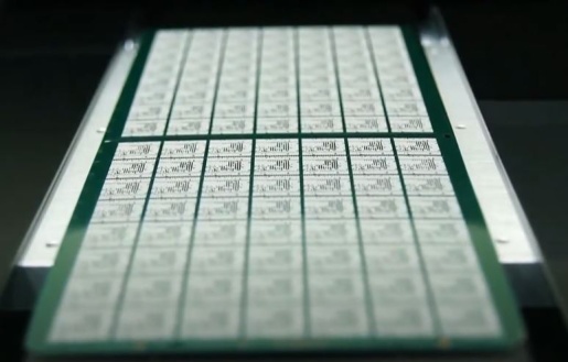
Anisotropic etching in circuit formation is a precision PCB and IC substrate manufacturing process used to define fine-line circuitry by selectively removing the surface copper layer. Unlike isotropic etching, anisotropic etching chemistries are engineered to etch at a significantly higher rate vertically than laterally, enabling highly accurate pattern transfer with minimal undercutting. This results in sharper line definition, improved dimensional control, and enhanced circuit density for HDI and advanced semiconductor packaging. By enabling precise copper patterning, anisotropic etching improves yield, signal integrity, and overall manufacturing reliability, making it essential for next-generation electronics in automotive, data center, industrial, and mobile applications.
Integrated Solutions
Our integrated circuit formation solutions span primary metallization through final finishes, optimizing PCB fabrication for improved reliability, signal integrity, and high-performance electronics manufacturing. Designed for HDI and advanced IC substrate applications, these chemistries enhance yield, reduce defects, and support sustainable production by improving process efficiency, minimizing waste, and enabling environmentally responsible, high-volume manufacturing across automotive, industrial, and semiconductor applications.
Sustainability
Our circuit formation technologies support sustainable PCB manufacturing by reducing hazardous material usage and minimizing water and energy consumption across metallization and finishing processes. Designed to help manufacturers meet Environment, Health & Safety (EH&S) and ESG goals, these advanced chemistries improve process efficiency, reduce waste, and enable high-performance, environmentally responsible production for HDI and IC substrate applications.
Reliability
Our circuit formation solutions deliver exceptional reliability through advanced copper adhesion promotion and innerlayer bonding technologies that ensure strong interconnect integrity throughout PCB fabrication. Engineered for high-performance HDI and IC substrate manufacturing, these chemistries improve mechanical durability, enhance signal integrity, reduce delamination risks, and support consistent, high-yield production for automotive, industrial, semiconductor, and data center applications.
Optimize PCB and leadframe chip packaging with our high-speed, clean ammoniacal etchants, improving performance for next-gen designs.
Learn MoreEnsure robust reliability for high-speed, low-loss applications with our wide range of engineered adhesion promoters.
Learn MoreAchieve MSL-1 performance and reliability with our adhesion promotors, from leadframe roughening to sidewall solderability enhancement.
Learn MoreOptimized molded interconnect device plating solutions that deliver precise selectivity, high yields, and ease of use.
Learn MoreAchieve a reliable foundation for superior PCB fabrication with our comprehensive chemistries, from dry film adhesion to final finish.
Learn MoreEnsure superior adhesion of solder masks and dry films with our solutions, delivering strong, reliable bonds.
Learn More