Explore Products for Wafer Bumping
Have a question? Let us help you.
We are here to help you. Please feel free to contact us with questions, comments or feedback.
Advanced wafer bumping metallization solutions enhance the reliability and performance of next-generation semiconductor packages.
Enhance wafer level packages with versatile wafer bumping solutions. Our tin, copper, and nickel metallization processes deliver exceptional uniformity and bond strength while eliminating voids, ensuring superior reliability and performance.
We are here to help you. Please feel free to contact us with questions, comments or feedback.
Enable advanced-node manufacturing with dual-damascene processes for bottom-up copper electroplating and void-free metallization.
Learn MoreOptimize pitch reduction, power efficiency, and reliability in advanced interconnect applications with our hybrid bonding solutions.
Learn MoreEnhance reliability in next-generation devices with our high-quality, sustainably sourced low-alpha tin materials.
Learn MoreUnlock best-in-class RDL performance with our RDL solutions, enabling efficient I/O pitch redistribution and advanced plating precision.
Learn MoreFill TSVs efficiently with our copper plating process, delivering reliable bottom-up plating for complex, high-density packages.
Learn MoreIntegrated Solutions
We are industry leaders in providing innovative, high-performance advanced interconnect metallization solutions that empower our customers to achieve superior results.
Sustainability
Our expertise and innovative interconnect metallization solutions are designed to support customers in achieving their Environmental, Health, and Safety (EH&S) objectives.
Reliability
Engineered for superior quality and performance, our solutions enable customers to achieve exceptional yield for complex packages.
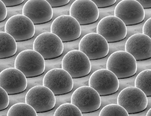
Wafer bumping is a process in semiconductor packaging where small metal bumps are added to the wafer surface, allowing for efficient chip-to-chip or chip-to-board connections. Our advanced metallization solutions in tin, copper, and nickel create uniform, flat bumps for reliable connections in wafer level packaging.
Our wafer bumping products include tin, copper, and nickel metallization solutions. These materials ensure excellent coplanarity, strong adhesion, and high conductivity, making them versatile for applications requiring durability and reliability in packaging.
Our wafer bumping electroplating solutions stand out due to their exceptional performance, ease of integration, and comprehensive technical support. We deliver industry-leading uniformity, coplanarity, and reliability, ensuring high-quality results even for the most advanced packaging applications. Additionally, our customer-focused approach includes dedicated support teams and tailored solutions, helping customers optimize processes and achieve their manufacturing goals with minimal risk and downtime.
By using uniform, coplanar bumps, our wafer bumping processes enhance electrical and mechanical stability. Our industry-leading metallization processes ensure high bond strength and void-free connections, which are critical for reliable, high-performance semiconductor applications.
Our wafer bumping metallization processes are designed for seamless integration into existing manufacturing lines, prioritizing ease of use and compatibility with standard equipment.