High-Throw DC
Create advanced mid-aspect-ratio boards with high-throw DC acid copper plating that boosts performance, reliability, and versatility.
Learn MoreAdvanced acid electrolytic copper metallization solutions for all applications, from ultra-high aspect ratio plating to filling the smallest blind microvias.
Optimize your Printed Circuit Board (PCB) designs with our production-proven electrolytic copper metallization processes and solutions, backed by industry-leading expertise and service. Enhance thermal conductivity, process control, and reliability across all features.
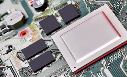

Advanced plating solutions enable complete and efficient filling of complex via, through-hole, and trench designs, ensuring optimal heat management.
Electrolytic copper solutions for conformal, high-aspect ratio plating of through-holes with excellent uniformity, enabling more complex board designs.
Advanced chemistries, engineered for precise and complete filling of complex features, ensure compliance with electrical design rules.
Our electrolytic copper metallization processes enable complex stacked microvia designs without compromising reliability.
Our user-friendly chemistries are designed for the manufacturing environment, featuring clear control specifications and human technical support when needed.
Create advanced mid-aspect-ratio boards with high-throw DC acid copper plating that boosts performance, reliability, and versatility.
Learn MoreEnsure reliable plating for thick, multi-layer PCBs with PPR solutions, offering uniform coverage of high-aspect-ratio through-holes.
Learn MoreOptimize your PCB designs with high-performance copper via filling solutions, engineered to tackle any metallization challenge.
Learn MoreIntegrated Solutions
Our integrated electrolytic copper metallization solutions enable high-performance PCB and IC substrate fabrication with superior via fill, conductivity, and reliability. Backed by industry-leading technical support, these advanced copper plating technologies improve manufacturing yield, reduce material and chemical consumption, and enhance process efficiency. Designed for sustainable electronics manufacturing, they help lower total cost of ownership while ensuring consistent, high-quality interconnect performance in advanced semiconductor and electronics applications.
Sustainability
Our electrolytic copper metallization solutions for advanced PCB and IC substrate manufacturing are designed for greater metal selectivity, reduced chemical and material waste, and higher manufacturing yields, supporting sustainable electronics production. By improving process efficiency, via fill performance, and deposition control, they help manufacturers lower environmental impact and total cost of ownership while ensuring high-reliability interconnect performance.
Reliability
Our electrolytic copper metallization solutions are proven to deliver high reliability in microvia, through-hole, and trench applications for advanced PCB and IC substrate manufacturing. Engineered for superior via fill, adhesion, and thermal stability, they ensure consistent electrical performance, reduced defect rates, and long-term interconnect integrity. These advanced copper plating technologies improve manufacturing yield and lower total cost of ownership in high-density electronic applications.

Electrolytic copper metallization is used in PCB and IC substrate manufacturing because it enables reliable electrical interconnection, superior via fill, and high-aspect-ratio feature plating required for advanced electronics. Copper plating is essential in manufacturing advanced printed circuit boards, and a well-designed and controlled electrolytic process provides the conductivity, adhesion, and uniform deposition needed to build today’s high-density, high-performance electronic devices. This technology improves signal integrity, thermal management, and mechanical durability while supporting higher manufacturing yields, reduced defect rates, and lower total cost of ownership. It is critical for enabling miniaturization and performance in automotive, computing, telecommunications, and semiconductor applications.
In high-density interconnect (HDI) PCB and IC substrate designs, electrolytic copper metallization enables precise, uniform plating of microvias, through-holes, and fine-line features essential for advanced electronics miniaturization. It ensures superior electrical conductivity, excellent via fill, and strong mechanical integrity, which are critical for high-reliability performance in compact layouts. This controlled copper deposition process improves signal integrity, thermal management, and interconnect durability while reducing defects and enhancing manufacturing yield. By supporting finer geometries and higher circuit density, electrolytic copper metallization helps manufacturers achieve lower total cost of ownership and consistent performance in automotive, computing, telecommunications, and semiconductor applications.
Electrolytic copper metallization improves thermal conductivity in PCB and IC substrate manufacturing by filling microvias, through-holes, and trenches with high-purity copper that creates efficient vertical and horizontal heat dissipation paths. This continuous copper network reduces thermal resistance, spreads heat away from active components, and helps prevent localized hotspots and overheating. As a result, it enhances device reliability, performance stability, and service life in high-power and high-density electronic designs. By improving heat management efficiency and reducing thermal stress on interconnects, electrolytic copper plating supports higher power densities, improved signal integrity, and lower total cost of ownership in advanced automotive, computing, and telecommunications applications.
Electrolytic copper metallization improves PCB reliability by delivering uniform, high-quality copper deposition that strengthens interconnect structures and ensures compliance with IPC standards for tensile strength, elongation, and resistance to V-pitting. This results in robust microvia, through-hole, and fine-line performance even in complex high-density designs. By enhancing adhesion, reducing void formation, and improving mechanical and electrical integrity, electrolytic copper plating increases manufacturing yield and long-term circuit stability. The result is more reliable high-performance PCBs with reduced field failures, improved signal integrity, and lower total cost of ownership in demanding automotive, aerospace, computing, and telecommunications applications.
In IC substrate manufacturing and advanced packaging, electrolytic copper metallization enables consistent, high-quality copper deposition for filling blind microvias, stacked vias, and X-vias, ensuring excellent coplanarity and low-profile trace formation for high-density interconnect (HDI) designs. This precise plating process supports fine-line circuitry, improves electrical conductivity, and enhances signal integrity in compact semiconductor packages. By delivering uniform via fill and strong adhesion, it increases manufacturing yield, reduces defects, and improves thermal and mechanical reliability. These benefits help enable advanced chip packaging performance while lowering total cost of ownership in high-performance computing, mobile devices, automotive electronics, and telecommunications applications.