Backside Metallization
Optimize via step coverage, yield, and reliability for power/RF with our solutions that integrate seamlessly with die attach material.
Learn MoreIndustry-leading compound semiconductor electroplating solutions and metallization / precious metal plating technologies are engineered for superior reliability, performance, and cost efficiency while accelerating time to market.
Enhance semiconductor performance with our precious metal plating solutions, designed to enable the fastest time to market at the lowest cost of ownership.
Our gold and palladium systems provide excellent fine-line capability, superior step coverage, and consistent electrical and mechanical characteristics.
Our gold electroplating solutions deliver exceptional capabilities for fine-line features, bump plating, via step coverage, and backside interconnect solutions.
Our non-cyanide deplate chemistry complements gold plating processes, delivering consistent gold etch results with minimal undercut of critical features.
Our palladium plating solutions offer excellent corrosion resistance, high thermal stability, and consistent material properties valued in Micro-Electro-Mechanical Systems (MEMS) manufacturing.
Our gold and palladium strike plating solutions enhance reliability by improving adhesion and minimizing contamination of subsequent metal layer steps.
Pure palladium pre-plating improves reliability and adhesion on passivated surfaces, such as nickel, that undergo subsequent soldering or die attach processing.
Optimize via step coverage, yield, and reliability for power/RF with our solutions that integrate seamlessly with die attach material.
Learn MoreAchieve superior bondability, reliability and thermal stability of display driver applications with our high-hardness gold solutions.
Learn MoreDesign next-generation Fan-Out Wafer Level Packaging (FOWLP) with our advanced gold and palladium solutions for thin metal films.
Learn MoreEnsure precise, uniform gold seed removal on TiW barriers with advanced, cost-effective gold etchants for semiconductor fabrication.
Learn MoreEnable high plating rates and superior step coverage with our advanced, cost-effective solutions for MEMS fabrication.
Learn MoreEnhance solderability and conductivity with high-purity deposits, seed filling, and adjustable roughness for advanced semiconductors.
Learn MoreIntegrated Solutions
Our complete range of pre-plate, strike and electroplating & metallization solutions ensure that you achieve superior results for your compound semiconductor applications.
Sustainability
We provide non-cyanide gold plating solutions to help our customers meet their Environment Health & Safety (EH&S) goals and maintain performance in compound semiconductor applications.
Reliability
Achieve unmatched corrosion resistance, high thermal stability and improved adhesion with our portfolio of compound semiconductor solutions.

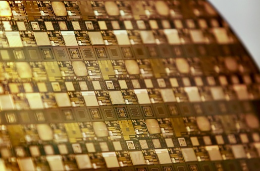
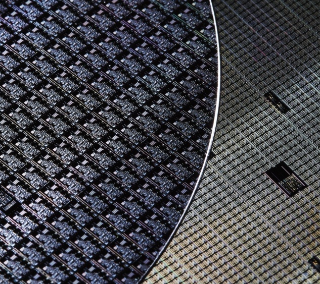
Compound semiconductor fabrication involves creating semiconductor products made from substrates containing multiple chemical elements. (i.e Gallium Arsenide, Silicon Carbide, & others). Compound semiconductors are most useful in applications such as Radio Frequency (RF), Power Integrated Circuits (IC's), Optoelectronics & Light-Emitting Diodes (LED's).
Challenges include fine-pitch patterning, step coverage into vias, thermal management, and achieving reliable interconnect surfaces. Advanced plating techniques enabled with materials like gold, palladium, and silver solutions can enhance the performance and durability of each die.
Electroplated gold features have a historic acceptance in compound semiconductor devices due to the material compatibility with the substrates, as well as advantageous material properties for low stress and thermal behavior. Our gold solutions enable fine line features, outstanding step coverage into vias, and favorable surface characteristics for backside interconnects and die attach.
Palladium plating enhances compound semiconductor fabrication by enabling superior adhesion of layers on top of metals such as nickel. Palladium also enables high reliability solderable finishes when gold is used as a topcoat. Palladium and palladium alloys offer MEMS devices unique and favorable mechanical and electrical characteristics.
Non-cyanide deplate technology reduces the operating costs in compound semiconductor fabrication by eliminating dangerous materials such as cyanide, Potassium Iodide (KI), or strong acids. Electrolytic deplate processing offers safer, more cost-efficient processing without compromising performance in gold plating applications.