Explore Products for Through-Silicon Via (TSV)
Have a question? Let us help you.
We are here to help you. Please feel free to contact us with questions, comments or feedback.
Fill TSVs efficiently with our copper plating process, delivering reliable bottom-up plating for complex, high-density packages.
Achieve defect-free TSV fills with MICROFAB® DVF-200, engineered for varying aspect ratios and high plating speeds. Ideal for evolving CMOS Image Sensors, Wafer-Level Chip Scale Package (WLCSP), and stacked memory, it meets the demands of complex, high-performance packages.
We are here to help you. Please feel free to contact us with questions, comments or feedback.
Enable advanced-node manufacturing with dual-damascene processes for bottom-up copper electroplating and void-free metallization.
Learn MoreOptimize pitch reduction, power efficiency, and reliability in advanced interconnect applications with our hybrid bonding solutions.
Learn MoreEnhance reliability in next-generation devices with our high-quality, sustainably sourced low-alpha tin materials.
Learn MoreUnlock best-in-class RDL performance with our RDL solutions, enabling efficient I/O pitch redistribution and advanced plating precision.
Learn MoreEnhance reliability and performance in next-generation semiconductor packages with advanced wafer bumping metallization solutions.
Learn MoreIntegrated Solutions
We are industry leaders in providing innovative, high-performance advanced interconnect metallization solutions that empower our customers to achieve superior results.
Sustainability
Our expertise and innovative interconnect metallization solutions are designed to support customers in achieving their Environmental, Health, and Safety (EH&S) objectives.
Reliability
Engineered for superior quality and performance, our solutions enable customers to achieve exceptional yield for complex packages.
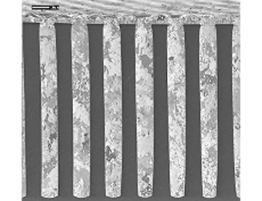
Through Silicon Vias (TSVs) are vertical interconnects that pass through a silicon wafer to enable 3D stacking and 2.5D integration, improving electrical performance, reducing interconnect length, and supporting higher integration levels in semiconductor devices.
MICROFAB DVF-200 is designed for fast, defect-free TSV filling with high-speed copper plating, supporting aspect ratios of 10:1. It is engineered to deliver uniform, void-free fills, meeting the stringent demands of 3D and 2.5D packaging applications.
Challenges in TSV filling include achieving void-free fills, ensuring uniform copper deposition, and managing high aspect ratios without defects. Advanced processes like MICROFAB DVF-200 provide solutions with high-speed plating and excellent reliability.
When selecting materials for TSV filling, it's essential to partner with a supplier that offers strong technical support. We stand out by providing in-depth expertise, helping customers optimize their TSV filling processes and overcome challenges efficiently, ensuring smooth integration into their production workflows.
MICROFAB DVF-200 systems are easily integrated into existing processes, as each system is a 3-additive solution that can be optimized to meet specific application requirements. This flexibility allows for tailored performance while maintaining a robust operating window, ensuring seamless integration and consistent results across various production environments.