Explore Products for Damascene
Have a question? Let us help you.
We are here to help you. Please feel free to contact us with questions, comments or feedback.
Empower damascene and dual-damascene processes to ensure bottom-up copper electroplating for void-free metallization.
Our ViaForm® products meet the precise demands of advanced-node manufacturing, delivering high-performance, void-free fills for complex interconnects, ensuring the reliability and scalability needed for cutting-edge semiconductor applications.
We are here to help you. Please feel free to contact us with questions, comments or feedback.
Optimize pitch reduction, power efficiency, and reliability in advanced interconnect applications with our hybrid bonding solutions.
Learn MoreEnhance reliability in next-generation devices with our high-quality, sustainably sourced low-alpha tin materials.
Learn MoreUnlock best-in-class RDL performance with our RDL solutions, enabling efficient I/O pitch redistribution and advanced plating precision.
Learn MoreFill TSVs efficiently with our copper plating process, delivering reliable bottom-up plating for complex, high-density packages.
Learn MoreEnhance reliability and performance in next-generation semiconductor packages with advanced wafer bumping metallization solutions.
Learn MoreReliability
Our damascene products enable void-free fills ensuring high reliability and enhanced performance for complex interconnects.
Integrated Solutions
We are industry leaders in providing innovative, high-performance advanced interconnect metallization solutions that empower our customers to achieve superior results.
Sustainability
Our expertise and innovative interconnect metallization solutions are designed to support customers in achieving their environmental, health, and safety objectives.

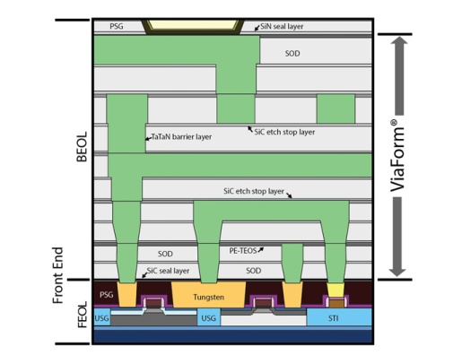
The damascene process is a technique for creating copper interconnects. Nanoscale vias and trenches are etched into a dielectric layer, followed by barrier and copper layer deposition, filling these patterns to create uniform, reliable interconnects in integrated circuits.
ViaForm products are widely used in dual-damascene processes for void-free, bottom-up copper fills. They provide precise control over copper electroplating, enhancing uniformity and reliability in high-density interconnects needed for advanced processing nodes.
We pioneered electroplating copper for damascene applications, with solutions that offer superior fill quality, consistency, and high throughput, backed by strong technical support and ongoing innovation.
ViaForm produces void-free copper interconnects with strong adhesion, ensuring long-term reliability under demanding conditions. Its precise copper filling reduces the risk of defects, enhancing durability in advanced Integrated Circuit (IC) substrates.
Yes, our damascene solutions are designed to scale effectively for high-volume manufacturing, ensuring consistent quality and performance.