Advanced Interconnect Metallization
Transform package performance with advanced interconnect solutions, delivering reliable, uniform, and robust results.
Learn MoreEmpower next-generation semiconductor packaging designs with our leading-edge metallization chemistry & material wafer level packaging innovations.
Our materials maximize semiconductor performance and reliability for next-generation technologies. With an agile and flexible development process, we deliver unique solutions that provide the lowest cost of ownership and the fastest time to market.

Our wafer level packaging solutions are uniquely tailored to each customer's application and performance requirements.
Our interconnect solutions deliver best-in-class reliability, improved electrical performance, and high first-pass yields for wafer level packaging applications.
Global collaboration, supported regionally by expert technical staff and centers of technological excellence.
Our offering includes the largest patent portfolio and most innovative range of solutions in advanced packaging and wafer level technology chemistry.
Transform package performance with advanced interconnect solutions, delivering reliable, uniform, and robust results.
Learn MoreEnhance reliability and performance in compound semiconductor fabrication with industry-leading precious metal plating technologies.
Learn MoreIntegrated Solutions
Our portfolio leverages advanced metallization chemistries and materials to enable cutting-edge semiconductor, wafer level packaging and Integrated Circuit (IC) substrates.
Sustainability
Polyfluoroalkyl Substances (PFAS)-free chemistries reduce environmental impact, supporting cleaner and safer manufacturing processes.
Reliability
High performance and enhanced reliability for advanced packages, driven by high-purity deposits, excellent uniformity, and optimized process throughput.
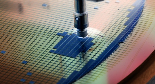
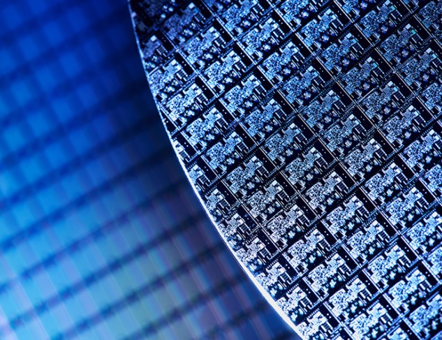
Wafer Level Packaging (WLP) is an advanced packaging method that integrates die and substrate fabrication at the wafer level. This approach enables miniaturization, better thermal and electrical performance, and higher reliability for high-density applications.
PFAS-free chemistries reduce the environmental impact of manufacturing processes by eliminating harmful substances from production. This helps companies comply with environmental regulations and create cleaner, safer products.
Our interconnect solutions offer best-in-class reliability, enhanced electrical performance, and high first-pass yields, ensuring efficient and high-quality outcomes for wafer level packaging applications.
We ensure high performance and enhanced reliability through high-purity deposits, excellent uniformity, and optimized process throughput, ensuring that your advanced packaging meets demanding industry standards.
Our solutions stand out with the largest patent portfolio in the industry, backed by cutting-edge metallization chemistries that enable superior wafer level packaging and IC substrates with improved performance and efficiency. We also customize our products to address the specific needs of each application, ensuring tailored solutions for every customer.