The innovative solutions that target impacts of AI in PCB manufacture and assembly
See the innovations reshaping PCB manufacturing for the AI era. Read the full article published by GlobalSpec here.
 GlobalSpec
GlobalSpec is a technology services company which provides a search engine of engineering and industrial products, indexing over 180 million parts divided into 2,300,000 product families, from over 24,000 manufacturer and distributor catalogs.
AI's pervasive influence across industries is significantly augmenting every modern application under the sun. At its core, AI leverages mathematical functions, such as convolutions, organized in layers to "learn." By processing application-specific datasets and training on unique inputs, AI systems can then accurately infer and output answers.
This escalating demand for AI technology has pushed embedded systems and AI-supporting infrastructures like supercomputers and data centers to their operational limits. Robust, power-dense processors are essential for meeting demanding computational requirements along with thermally aware layout and design practices.
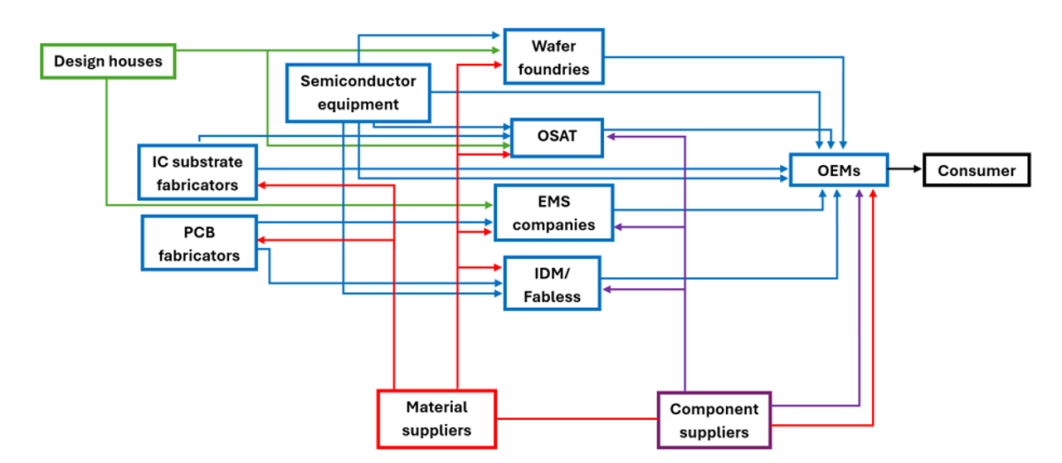
This necessitates a combination of innovative silicon and fabrication techniques, advanced packaging and precision circuit board fabrication and assembly, which challenges the entire electronics manufacturing supply chain (Figure 1).
PCB fabricators and electronic manufacturing services (EMS) must adapt to custom board layouts, high-speed interconnects and thermal-aware assembly for AI servers and edge devices.
The move toward exascale computing
High performance computing
High-performance computing (HPC), also known as supercomputing, involves combining processing power to solve complex computational problems. HPC has always relied on high-performance accelerators that feature on-chip parallelism to achieve considerable data reuse. At the rack-level, HPC installations house separate servers that are connected by a high-speed communication network, which turn the set of servers into a larger compute cluster, or supercomputer.
The tightly coordinated infrastructure of HPC is optimized to run extraordinarily complex simulations. Researchers globally have already upped the ante in the move toward exascale computing, with supercomputers that can perform less than 1018 floating-point operations per second (FLOPS). This can be used to solve intricate real-world problems, including:
- The identification and reverse engineering of microbes to produce uniquely effective antibiotics
- Building and testing large-scale reactors to speed up the design and development of carbon capture technologies
- Performing accurate simulations of the motion and interactions of atoms and molecules to advance human knowledge of molecular dynamics
- Creating computational models of ground motion during an earthquake to enable engineers to discern areas most at risk for a severe earthquake.
Data center
While conventional HPC applications have been built to support AI workloads, traditional data centers are now seeking to be more AI-optimized. The infrastructural demands of AI have skyrocketed in recent years, particularly with the growing popularity of generative AI, which has led to the extensive use of multimodal large language models (MLLMs) such as ChatGPT, DeepSeek, Gemini and others. The resource demands are staggering when considering how frequently people use AI each day — and then multiply that by the entire population served by a data center. This can range from a few hundred users for enterprise, edge and colocation data centers to millions with cloud facilities and hyperscalers. While more traditional data centers run distributed applications that rarely require server synchronization, there is some overlap between HPC and data centers.
For one, the resource demands of AI have also moved data centers toward exascale computing. Optimizing both HPC and data centers for AI workloads calls for power-hungry GPUs en masse to meet traffic demands. Furthermore, training the complex deep learning models with massive datasets is also a monumental task, often relying on a cluster of interconnected racks (i.e., supercomputers). This puts a great deal of strain on the entire data center infrastructure from the facility level to the racks, and down to the chips.
Power and thermal
Challenge
HPC and data center GPUs often leverage complex microarchitectures that support hundreds of billions of transistors, utilizing highly advanced process nodes (4 nm or 5 nm) designed to meet the needs of AI workloads. These processors are extremely power-hungry; Intel’s Max Series (used in the Aurora exascale supercomputer), for example, uses up to 600 W, while NVIDIA’s Blackwell consumes up to 1,000 W (G200). This is not just a challenge at the semiconductor level but also at the system level. As a result, rack power density has increased from the standard 5 kW to 10 kW to over 100 kW in AI-optimized data centers and HPCs.
The first challenge is simply delivering power to the multitude of cores housed within a rack. Data centers have recently transitioned from 12 V power rails to 48 V to meet the increasing power demands of AI. The voltage rail will continue to rise with continually rising compute demands. Power-dense (often Gallium Nitride (GaN-based)) power supply units (PSUs) supply power to the AI cards via vertical (or lateral) power delivery modules. These modules are optimized to deliver the high amperage required for GPUs, in the order of thousands of amps.
Solution
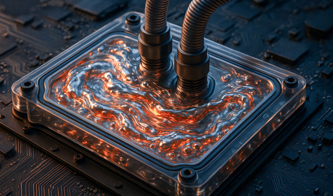
Thermal management is one of the biggest challenges limiting progress in high-density compute infrastructure. The task of removing this heat must go beyond the conventional forced air cooling that data centers have traditionally relied upon. In reality, as data centers and HPC move up toward exascale computing, chip hotspots can no longer be effectively addressed without liquid cooling. Technologies like direct-to-chip (DTC) and immersion cooling are now necessary over forced air convective cooling to meet the required power dissipation per square centimeter, often ranging from 50 W/cm² to 100 W/cm².
DTC cooling relies heavily on several key technologies:
- The microchannel coldplate, generally copper-based, circulates coolant via flow channels that will sometimes contain turbulators to maximize heat transfer
- An inlet and outlet arrangement optimized for heat transfer and minimizing unwanted interactions between liquid jets
- The dielectric-based liquid coolant absorbs heat from the component and sends it to the coolant distribution unit (CDU)
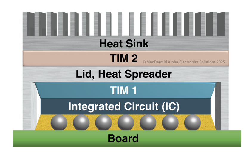
- The thermal interface material (TIM) is used to minimize thermal resistance (Rth) between surfaces and conduct heat from either the AI card’s heat spreader (packaged) or the lidless bare die to the coldplate (Figure 3)
From a PCB-assembly (EMS) materials perspective, TIMs are the primary consideration. Several factors could impede heat transfer, including surface flatness and roughness at the interface, CTE mismatch between the AI package or bare die and the coldplate, contact pressure variations, and surface contamination: impacting Rth.
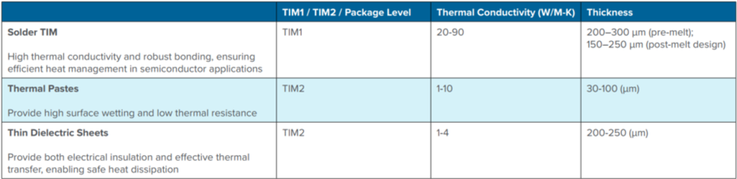
Solder-based, or sintered, TIMs (sTIMs), also known as TIM1, are ideal for DTC cooling due to their high thermal conductivity for bare die, lidless semiconductors. Often indium-based, sTIMs are formulated to minimize Rth and enhance the thermal conduction path due to their high isotropic thermal conductivity and enhanced wetting and fine-feature compatibility. These materials are designed for high thermal cycling durability, a high CTE with low modulus and strong adhesion — properties that are critical for compact, high-density HPC and data center applications.
Polymer-based TIMs (TIM 1.5 and TIM2) either used between bare die and heatsink or between lid/heatspreader and heatsink – while exhibiting a lower thermal conductivity than TIM1 – are relatively soft and pliant, absorbing the thermomechanical strains that come from mismatched CTE at the interface. Table 1 demonstrates the options available for TIMs materials. The advice is that a designer should choose the thinnest solution possible to fill the thermal interface.
High-speed digital
Challenge
High-speed communication links such as NVLink, InfiniBand and PCIe are essential for transmitting and receiving vast volumes of AI data at the PCB level. This drives the need for high-density interconnect (HDI) PCBs. Memory modules using newer double data rate (DDR) generations also rely on HDI designs. Compared to standard multi-layer boards, HDI PCBs are significantly more complex to manufacture, requiring multiple lamination cycles and precision laser-drilled stacked microvias. Modern HDI layouts incorporate a wide variety of via types and aspect ratios — from plated-through holes to microvias. The increased via density, along with finer features such as tightly spaced components and high pin-count packages, has pushed line width and spacing (L/S) requirements down to 25/25 µm, with many designers now targeting 20/20 µm, and some even attempting 15/15 µm. L/S below 15/15 µm is currently seen primarily in IC substrate technologies.
This puts pressure on fabricators that could previously rely on subtractive manufacturing processes that yield 50/50 µm L/S. Instead, semi-additive processing (SAP) or modified SAP (mSAP) can be used to create the fine line patterning now required in HDI. So, instead of plating an entire surface with copper to then pattern with photoresist and etch away, the copper is deposited on top of the patterns to the desired thickness. This has become a necessary evolution in PCB manufacturing, centered around the integrity of processes for making holes conductive — commonly known as primary metallization, which enables subsequent electroplating by way of a conductive seed layer.
Solution
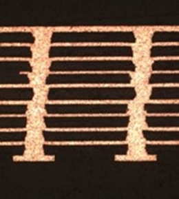
Traditionally, electroless copper is used to deposit the metallization seed layer before building up thickness; however, a palladium layer used before the main copper plating can lead to interfacial defects and separation of the target pad (Figure 5). These problems only become more pronounced with microvias.
Direct metallization (DM) is an alternative process that begins with conditioning the surface, coating it with a carbon or graphite material and micro-etching to remove the carbon particles from the copper areas (including the target pad). Since there is a direct bond between the base copper and electroplated copper, there are far fewer interfacial defects, resulting in higher via and board reliability. High reliability is more critical in PCBs and assemblies that are thermally challenged, as HPC and data centers often are.
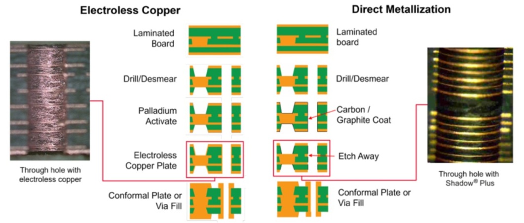
Furthermore, the low-etch DM technology was developed to meet the needs of mSAP. DM is compatible with all electrolytic copper plating systems, including direct current (DC), periodic pulse reverse (PPR) and copper via fill. DM is particularly important for new via fill processes that go beyond the conventional conformal plating baths, preferentially plating into a variety of via sizes. Conformal via filling will plate 1:1 with the surface copper, while via fill chemistries plate at faster rates in the vias, compared to the surface.
Shown in Figure 6, these via fill chemistries help increase the capability of board designs with complex via structures, such as stacked vias, staggered vias and any-layer build-up vias that need to be filled. In other words, via fill technology can simultaneously perform both via filling with a high filling performance and TH plating with a reliable deposit for mSAP, with minimal surface copper build-up.
Speed, scalability and sustainability
Challenge
Data center and HPC operators face growing pressure to support global manufacturing, maintain agile supply chains and accelerate time-to-market for AI hardware platforms. These demands are further complicated by sustainability goals, shifting power availability from local grids, and the integration of renewable energy sources through power purchase agreements. As AI workloads expand, so do the demands on power, water and land — creating constant pressure to minimize resource consumption while scaling infrastructure.
In addition, sustainability goals have become more critical to PCB fabrication, the OEMs and the EMS network. Goals include reducing the use of hazardous substances and precious metals in the manufacturing process for environmental, health and safety (EHS) compliance. PCB fabrication and assembly is always challenged to maximize process efficiency and reduce costs, all while staying relevant and meeting the needs of next-generation technologies that may call for the use of upgraded laminate materials, ultra-thin L/S and increasingly higher aspect-ratio vias.
Solution
These needs require a closer look at the entire materials supply chain. Material compatibility within existing manufacturing processes is key in optimizing scalability, efficiency and reliability while reducing costs. Curing temperatures, pressure requirements, minimum and maximum tolerances and many more considerations must be assessed to connect, reinforce, protect and manage heat in electronic components. As much as possible, the materials used must be optimized for reworkability and repairability to reduce waste and improve yield in fast-paced production environments.
From a sustainability standpoint, processes like DM deliver measurable reductions in water, power, chemical consumption and waste treatment compared to electroless copper processes, and by eliminating hazardous materials like formaldehyde and removing the necessity of precious metals like palladium.
Low-temperature lead-free solders are another powerful technology to enable greener circuit assembly operations. By decreasing reflow temperatures from 250° C to temperatures as low as 175° C, EMS companies can cut energy consumption by more than 30% per production run.
Using more bio-based materials in polymers — such as those found in underfill reinforcement, conformal coatings and potting compounds — helps replace oil-based alternatives. This shift supports compliance with EHS standards and promotes environmentally friendly circuit protection.
Conclusion
The processing and power burden of AI puts pressure on the entire electronics supply chains from semiconductor to system. The most significant impact for EMS is from a materials perspective, where enhanced thermal management must be maintained despite the increasing density of the boards. This means that materials to connect, reinforce, protect and manage heat in electronic components must be process-ready for scalability and PCB reliability, and reworkable to increase yield. For PCB fabricators, direct metallization technology enhances HDI fabrication and account for the necessary newer mSAP.
MacDermid Alpha is uniquely positioned to meet these needs. They offer a broad portfolio across circuit board assembly, board-level interconnects and thermal management, with a strong emphasis on process compatibility and reliability. For example, reworkable materials commonly used in PCB assembly processes, such as edge bonding, are offered through MacDermid Alpha to ensure lower prototyping costs.
Their established technical teams helps both fabricators and assemblers achieve high first-pass yields, thermal/electrical performance and design enablement. All of these factors combined allow higher I/O counts and smaller nodes, all while ensuring best-in-class reliability and electrical performance. For more information, contact MacDermid Alpha Electronics Solutions.
Have media inquiries?
Connect with Us
For all media inquires, please contact Joanna Locke, Public Relations Manager
Email us