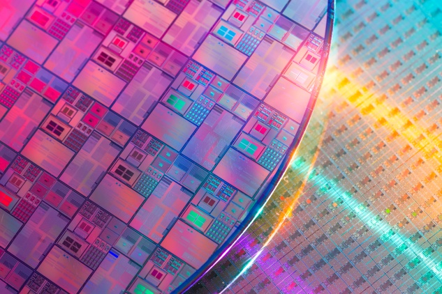
NOVAFAB® NANOTWIN Cu
A high-purity copper electroplating process formulated for fabricating pillars or pads for hybrid bonding applications.
Contact UsProduct Overview
NOVAFAB NANOTWIN Cu is a high-purity copper electroplating process which produces a <111> oriented deposit with a high fraction of nano-twinning. It is specially formulated for the fabrication of pillars or pads for wafer level packaging applications that require hybrid bonding. It enables low temperature, high reliability copper to copper interconnects for Die-to-Die (D2D), Die-to-Wafer (D2W), and Wafer-to-Wafer (W2W) bonding.
Product Features
Novel One-Part Additive System
NOVAFAB NANOTWIN Cu is a ready-to-use solution designed for use with soluble or insoluble anodes and produces a <111> oriented crystal structure.
Excellent Process Stability
The NOVAFAB NANOTWIN Cu process yields excellent thickness distribution over the whole wafer surface for consistent electrical properties and bondability.
Highly Nano-Twinned Columnar Copper
Nano-twinned Cu (nt-Cu) demonstrates superior mechanical and electrical properties. High-performance applications are driving reductions in I/O pitch and increases in I/O density, leading to solder removal at smaller pitch sizes. NOVAFAB NANOTWIN Cu exhibits high nanotwin density, producing high-purity deposits, excellent process stability, and a wide operating window.

Featured Applications
Hybrid Bonding
D2D, D2W, and W2W hybrid bonding for sub 40µm pitch packages enables 3D and chiplets, resulting in improved circuit efficiency and reduced power consumption.
Product Documentation
No Documents Found
We can't seem to find the documentation right now. Please reach out to us and we'll get what you're looking for.
Contact us