NOVAFAB® Fine Grain Copper
Award-winning advanced electroplating process producing a unique, ultra-pure, copper film for hybrid bonding applications.
Contact UsProduct Overview
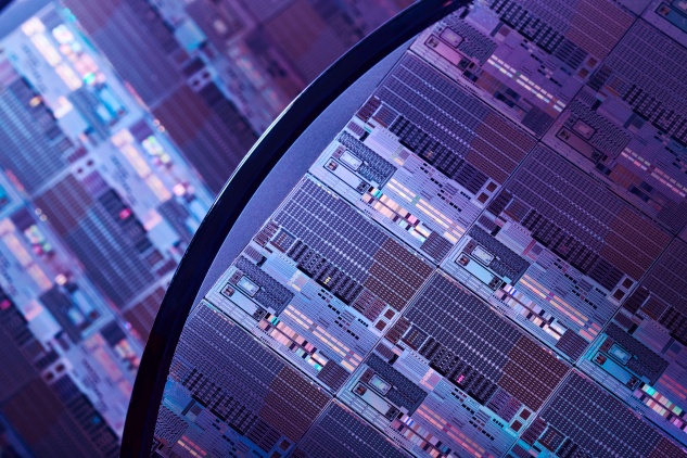
The award-winning NOVAFAB Fine Grain Copper electroplating process produces a unique film that supports the mechanical and electrical requirements of advanced semiconductor packaging. Engineered for various wafer-level packaging applications, NOVAFAB Fine Grain Copper excels in hybrid bonding.
The technology maintains a stable grain structure throughout production and demonstrates controlled grain-growth at post-processing temperatures, ensuring excellent bonding at the interface. This system enables high-quality and high-reliability interconnects for Die-to-Die (D2D), Die-to-Wafer (D2W) and Wafer-to-Wafer (W2W) bonding.
Product Features
Improved Device Performance and Reliability
NOVAFAB Fine Grain Copper produces a high-density, ultra-pure deposit that minimizes signal degradation, improving overall device performance and reliability.
Stable Grain Structure for Defect-Free Bonding
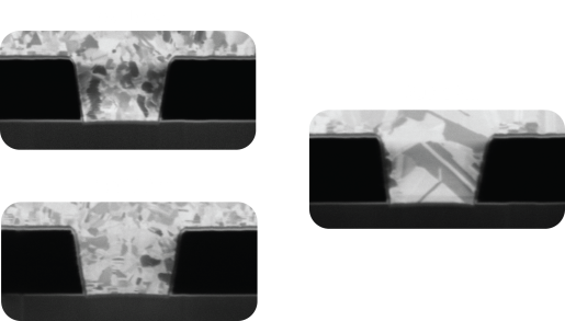
Grain size is maintained through processing and controlled grain growth during annealing, ensuring the formation of defect-free bonds, significantly enhancing quality and reliability.
Adaptable Copper Deposit for Small Features
With a <0.2μm grain size, the copper deposit is adaptable for small features, making it ideal for applications requiring high-density interconnects with advanced mechanical and electrical demands.
Innovative Copper Electroplating Process Ensures Reliability of HDI
NOVAFAB Fine Grain Copper enables controlled grain growth during annealing, ensuring the formation of defect-free bonds, significantly enhancing quality and reliability. The ultra-pure copper film minimizes signal degradation, improving overall device performance and reliability. With a <0.2μm grain size, the copper deposit is adaptable for small features, making it ideal for applications requiring high-density interconnects with advanced mechanical and electrical demands.
MacDermid Alpha’s Fine Grain Portfolio
Award-winning NOVAFAB Fine Grain Copper represents the latest innovation in our Fine Grain Portfolio, designed to address key challenges in heterogeneous integration and hybrid bonding.

Featured Applications
Hybrid Bonding
NOVAFAB Fine Grain Copper excels in hybrid bonding. The technology maintains a stable grain structure throughout production and demonstrates controlled grain-growth at post-processing temperatures.
D2D, D2W and W2W Bonding
This system enables high-quality and high-reliability interconnects for Die-to-Die (D2D), Die-to-Wafer (D2W) and Wafer-to-Wafer (W2W) bonding.
Download
Product Documentation
No Documents Found
We can't seem to find the documentation right now. Please reach out to us and we'll get what you're looking for.
Contact us