Direct Metallization: A Game-Changer for the Electronics Industry
Want a smarter, more sustainable alternative to electroless copper? Read this article to learn how direct metallization delivers.
 Harry Yang
VP Commercial Asia, Circuitry Solutions
MacDermid Alpha Electronics Solutions
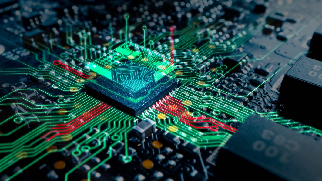
Direct metallization is an advanced manufacturing process used in the fabrication of printed circuit boards (PCBs) and integrated circuit (IC) substrates. It efficiently deposits a conductive layer onto non-metallic surfaces. This technique is becoming popular in PCB fabrication for smartphones and handheld devices, improving production efficiency and yield. It replaces traditional electroless copper processes, which rely on hazardous chemicals like formaldehyde. Direct metallization improves quality, reduces defects, and offers a more sustainable solution for the electronics industry.
Direct metallization provides fabricators with an opportunity to enhance supply chain resilience by improving process efficiency, reducing reliance on hazardous and tightly regulated chemicals, and lowering overall material consumption. Its environmentally responsible chemistry and streamlined workflow reduce waste and energy use, supporting both sustainability goals and a more agile, future-ready supply chain.
As demand for miniaturization and high-performance devices grows, direct metallization is crucial for manufacturers to stay competitive in fabrication and meet their environmental goals.
Supply Chain Management in the Electronics Industry: A Broader Perspective
In the electronics industry, supply chain management often focuses on components and semiconductors. This narrow focus can miss critical risks in electronics production. Two often underestimated factors - manufacturing capacity and access to essential materials – are becoming increasingly crucial. These challenges are pronounced in semiconductor manufacturing and packaging/substrate production. A comprehensive supply chain approach is essential for resilience and stability in electronics manufacturing.
Semiconductor manufacturing is diversifying geographically, but cost-effective processing for IC substrates and high-density interconnect (HDI) PCBs remains limited. Manufacturers now prioritize consistent availability of critical materials and processing capacity to mitigate any supply chain risks. An agile processing approach will:
- Strengthen risk management.
- Enable quicker supplier transitions.
- Improve overall supply chain resilience.
Electroless Copper Plating
Electroless copper plating is widely used, especially for high-aspect-ratio through hole and small blind via processing. It works for less complex designs but becomes problematic as feature sizes shrink. Smaller line and space requirements tighten the process control, reducing etch rate, which is difficult to do with standard electroless copper. This issue is pronounced in more difficult designs, such as advanced HDI PCBs and IC substrates.
Several supply chain factors are associated with electroless copper plating:
- Metal Precursors – The process relies on palladium and copper for activation, with prices fluctuating depending on market conditions.
- Defect Rates – Smaller hole diameters increase defect rates, requiring strict quality control to reduce scrap, becoming more critical as the cost of boards go up.
- Resource Consumption – Electroless copper plating demands higher water and energy consumption and involves the use of hazardous chemicals. This makes it a less viable solution in regions with strict environmental regulations.
Managing hazardous waste is essential in the circuit board fabrication supply chain, where disposal challenges can disrupt operations and increase costs. To ensure a responsible and efficient supply chain, manufacturers must:
- Implement robust waste management protocols.
- Partner with certified waste disposal firms.
- Prioritize waste minimization strategies.
By embedding these practices into their operations, manufacturers can strengthen compliance, reduce costs, and support broader sustainability goals.
The Rise of Direct Metallization
Direct metallization effectively addresses these challenges in fabricating advanced HDI PCBs and IC substrates. It reduces reliability issues such as voids and microvia defects, by limiting quality control inconsistencies compared to electroless copper plating. This leads to lower scrap rates and better cost predictability. Its simplified processing and material availability give manufacturers flexibility, smoother supplier transitions, and better supply chain resilience and control.
Flexibility and Compatibility of Direct Metallization
Direct metallization simplifies fabrication and is compatible with various substrate materials, including:
- Standard FR4 laminates.
- BT epoxy core layers.
- Polyimide.
- Ajinomoto buildup film (ABF).
- Reinforced and unreinforced PTFE.
- Resin-coated copper (RCC).
- Liquid crystal polymer (LCP).
This broad compatibility helps prevent material availability from becoming an added supply chain risk, which enables efficient production across a wide range of products.
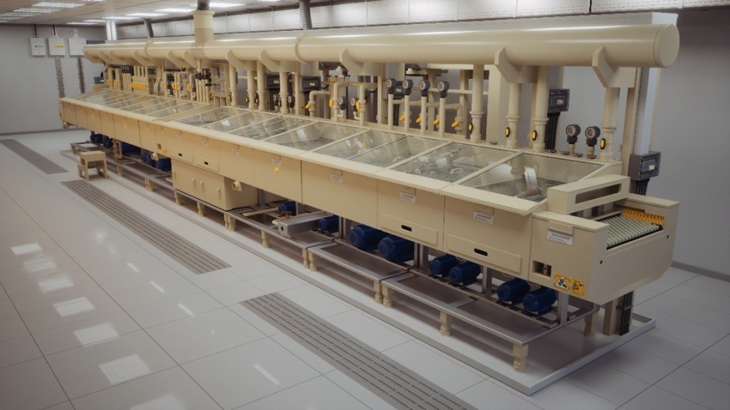
Additionally, direct metallization is compatible with most existing electrolytic copper plating systems without any modifications. This enables efficient production across a wide range of products, supporting supply chain resilience and adaptability.
Benefits of Direct Metallization
Key advantages:
- Versatility – Supports both advanced HDI designs and traditional double-sided PCBs, allowing one production line to handle diverse products.
- Higher Yields – Non-dynamic chemistry reduces defect rates and boosts production efficiency, improving overall output.
- Increased Manufacturing Capacity – Expands production capacity for HDI designs and IC substrates.
- Lower Supply Chain Risks – Eliminates reliance on costly materials and hazardous chemicals while ensuring broader material compatibility.
- Process Efficiency – Seamlessly integrates into existing electrolytic copper plating systems, including horizontal processing lines.
- Reduced water consumption – Direct metallization reduces water usage by over 70%, making it a more environmentally friendly alternative.
Direct metallization improves cost management by increasing yields through a stable, non-dynamic chemistry that reduces defects and boosts production efficiency. It also lowers supply chain risk by eliminating reliance on costly, hazardous materials and enabling compatibility with a wider range of substrates. Direct metallization offers greater reliability, efficiency, and supply chain resilience, making it a standout choice for manufacturers to enhance production and reduce risks.
Direct Metallization: A Key Advantage in Advanced Electronics Manufacturing
In today's volatile supply chain, constraints on production capacity and material availability are among the most challenging concerns. Semiconductor manufacturing is diversifying geographically, with advanced HDI PCB and IC substrate fabrication experiencing accelerating growth. Direct metallization enables efficient, adaptable manufacturing for IC substrates and advanced HDI PCBs. It streamlines processing, reduces dependence on costly and hazardous materials, and supports faster production transitions.
Unlike electroless copper, which has higher defect rates, complex waste disposal, and resource-intensive processing, direct metallization offers better material compatibility, improved yields, and reduced supply chain risks. Its ability to support high- and mid-complexity designs on a single production line makes it a strategic choice for manufacturers in today's competitive electronics landscape.
To learn more about direct metallization for HDI PCBs and IC substrates, please contact us here.
Have media inquiries?
Connect with Us
For all media inquires, please contact Joanna Locke, Public Relations Manager
Email us