Direct Metallization: A Future-Ready Solution for Advanced Electronic Applications
Read this article and find out how direct metallization makes PCB manufacturing more sustainable, efficient, and cost-effective.
 Mark Edwards
Strategic Account Director – Circuitry Solutions
As market dynamics shift, the need to geographically diversify electronics manufacturing is more pressing than ever. Companies are setting ambitious sustainability goals, implementing production processes that minimize environmental impact without compromising high performance and reliability. Direct metallization (using graphite, carbon, or polymer-based materials) is a key PCB process that supports these goals. Besides engineering advantages, it offers cost savings and competitive benefits. Integrating direct metallization is a strategic investment for companies upgrading or installing new fabrication operations, driving efficiency and long-term success.
Primary Metallization – The Foundation of PCB and IC Substrate Manufacturing
All circuit boards and IC substrates depend on inner layer connections, commonly created by buried through holes or microvias. This allows electrical signals to pass between components. Fabricators form vias mechanically or with laser drilling, then plate them with copper for conductivity.
Primary metallization is essential for this process, preparing non-conductive hole walls for copper electroplating, often called “making holes conductive.” It ensures reliable performance in both standard multilayer circuits and complex high-density interconnect (HDI) designs with blind and stacked vias. With growing demand for reliability and efficiency, fabricators and OEMs prioritize sustainability, higher yields, and stronger supply chains.
Currently, the PCB industry utilizes two different processes for primary metallization:
Electroless Copper (Traditional Method)
- Uses a chemical reducing agent, such as formaldehyde.
- Involves multiple chemical baths for cleaning and plating.
- Requires a palladium/tin catalyst to initiate and accelerate deposition.
- Chemically deposits a thin copper layer on via hole walls for subsequent electroplating.
Direct Metallization (Advanced Alternative)
- Eliminates several time-consuming processing steps.
- Deposits a conductive coating onto via hole walls for subsequent electroplating.
- Greatly reduces water, energy, and chemical use compared to electroless copper plating.
Key Benefits of Direct Metallization
While direct metallization is well-suited for standard circuit board fabrication with large via hole sizes, its greatest benefits emerge in advanced applications such as IC substrates and HDI circuit boards.
With continuous enhancements, including fine particle size, direct metallization handles high-aspect ratio holes and microvias, offering these key benefits:
- Direct copper-to-copper bonding, eliminating the need for palladium-based interfaces.
- Improved reliability of the electroplated copper layer.
- Enhanced epitaxy and grain structure, particularly within microvias.
- Higher production yields through a streamlined manufacturing process.
Direct metallization is compatible with a wide range of dielectric (substrate) materials and feature sizes. It supports FR4 materials for consumer electronics, PTFE laminates for high-frequency telecom and radar, and ultra-thin resin films for HDI builds. This versatility makes it ideal for industries like automotive, aerospace, telecommunications, data centers, and consumer electronics, all of which demand reliability and high performance.
Direct Metallization – Enables Cost-competitive and Sustainability Advantages
Companies diversifying their PCB manufacturing must navigate complex environmental regulations affecting cost competitiveness and supply chain risks.
In this context, direct metallization stands out as a superior, sustainable, and cost-effective alternative to electroless copper plating. It offers key environmental and operational benefits, including:
- Up to 90% reduction in rinse water consumption and operator labor costs.
- No continuous generation of by-products in the process tank.
- Elimination of precious metal precursors such as palladium.
- Removal of hazardous chemicals, such as formaldehyde.
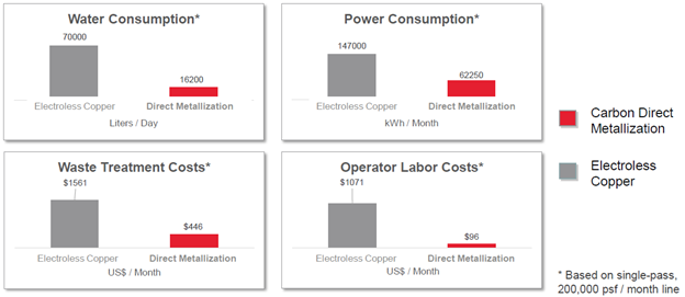
These advantages translate into significant savings in water, waste treatment, power, chemical, and labor costs. The charts below provide a comparison of these metrics for a single-pass production line, using Blackhole® direct metallization and Via Dep® 4550 electroless copper, operating at 200,000 panel sq.ft./month.
Direct metallization also helps mitigate supply chain risks. Reducing the environmental footprint gives manufacturers more flexibility in choosing production sites, reducing their vulnerability to material, water, labor, and energy shortages. As companies prioritize sustainability and environmental regulations tighten, direct metallization allows manufacturers to remain compliant without compromising cost, efficiency, or quality.
A Sustainable and Competitive Path Forward
As the electronics industry navigates the complex challenges of geographic diversification, direct metallization stands out as a scalable, efficient, and future-ready solution. By streamlining PCB manufacturing processes and reducing environmental impact, it supports regional expansion strategies while maintaining quality, cost control, and mitigating supply chain risks. These advantages are critical in the production of advanced HDI circuit boards and IC substrates used in aerospace, automotive, consumer electronics, and telecommunication applications.
To learn more about direct metallization for HDI PCBs and IC substrates, please contact us here.
Have media inquiries?
Connect with Us
For all media inquires, please contact Joanna Locke, Public Relations Manager
Email us