Application Overview
Typical wafer level packaging involves a multitude of processes, including redistribution lines, copper pillars and solder bump formations for both Fan-in and Fan-out wafer level applications.
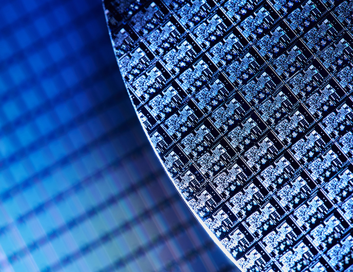
Wafer Level Packaging (WLP) involves the forming of interconnects on either traditional silicon wafers or polymer-based reconstituted wafers.
Typical wafer level packaging involves a multitude of processes, including redistribution lines, copper pillars and solder bump formations for both Fan-in and Fan-out wafer level applications.
For additional details, please visit the product page.
For additional details, please visit the product page.
Please see the solutions page for details.
Please see the solutions page for details.
For additional details, please visit the product page.
For additional details, please visit the product page.
Please see the solutions page for details.
Please see the solutions page for details.