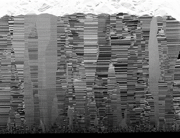
NOVAFAB NANOTWIN Cu – Bump-less
Nano-twinned Cu (nt-Cu) demonstrates superior mechanical and electrical properties and has drawn a lot of attention in the wafer-level packaging (WLP) field for Cu to Cu direct and hybrid bonding. D2D, D2W applications and redistribution line (RDL) anti-cracking can benefit from improved electromigration resistance. Performance and thermal demands driving I/O pitch reduction and I/O density increases lead to solder removal at reduced pitch size.
- 111 oriented crystal structure.
- Highly stable one-part novel additive system.
- High speed deposition.
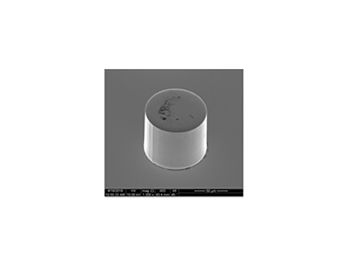
MICROFAB SPM-1100
MICROFAB SPM-1100 copper plating solution demonstrates superior high-speed plating and coplanarity in a KV low system which provides exceptional within-wafer, within-die, and within-feature uniformity. MICROFAB SPM-1100 is a next generation high speed solution and is a perfect replacement for industry leading MICROFAB SC copper solutions where >COP and plating rate is desired. It is also perfectly mated with our boric acid free nickel barrier, MICROFAB EVF NiBar and tin silver solutions MICROFAB TS-650
- Flat bump shape.
- Excellent coplanarity.
- High speed deposition.
View Products in Plating - Copper
- Damascene
Superior Filling Performance for Wafer Fabrication
- Custom solution packages based on the latest ViaForm products through our close customer collaborations
- Capable of meeting manufacturing needs of the most advanced processing nodes
- Pioneering advanced Cu technologies with proven uniform interconnect fill and superior reliability
- MICROFAB® SPM-1200
MICROFAB SPM-1200 copper plating solution demonstrates superior coplanarity in a KV low system which provides exceptional within-wafer, within-die, and within-feature uniformity.
- Good WID, WIF
- Excellent coplanarity
- High throughput
- Flat bump shape
- Low voiding
- MICROFAB® SPM-1100
MICROFAB SPM-1100 copper plating solution demonstrates superior high-speed plating and coplanarity in a KV low system which provides exceptional within-wafer, within-die, and within-feature uniformity.
- Pillar / Post
- Excellent coplanarity
- High speed
- High throughput
- Flat bump shape
- Low voiding
- NOVAFAB® Nanotwin Cu
Copper electrodeposited with a nano-twinned crystal orientation demonstrates superior mechanical and electrical properties and has drawn a lot of attention in the wafer-level packaging (WLP) field for Cu to Cu direct and hybrid bonding, including D2D, D2W, W2W applications. Additionally, fine line redistribution layers (RDL) plated with NOVAFAB Nanotwin Cu can benefit from improved mechanical reliability and electromigration resistance.
- Novel one-part additive system
- <111> oriented crystal structure
- High nanotwin density
- Excellent process stability
- Wide operating window
- High purity
- MICROFAB® CU1000
Higher speed copper plating process for copper pillar in flip chip package, copper microbump in 3D interconnect package as well as redistribution layer. The process delivers accurate bump height uniformity and bump shape control.
- High speed
- Excellent coplanarity
- Ease-of-use
- MICROFAB® CUMSA100
MICROFAB CUMSA100 enables high plating rates for high throughput leading to a lower cost of ownership. This is enabled through a low consumption additive and simple and easy bath maintenance.
- Wide operating window
- High purity
- Ease-of-use
- Low voiding
- MICROFAB® SC-50
High speed copper plating process for copper pillar in flip chip package, copper microbump in 3D interconnect package as well as redistribution layer. The process delivers accurate bump height uniformity and bump shape control.
- High speed
- Good coplanarity
- Versatility
- Ease-of-use
- High throughput
- MICROFAB® SC-40
High speed copper plating process for copper pillar in flip chip package, copper microbump in 3D interconnect package as well as redistribution layer. The process delivers accurate bump height uniformity and bump shape control.
- High speed
- Good coplanarity
- Versatility
- Ease-of-use
- High throughput
- MICROFAB® SC-32
Copper plating process for copper pillar in flip chip package, copper microbump as well as redistribution layer. The process delivers accurate bump height uniformity and bump shape control with higher plating rates than MICROFAB SC.
- Good coplanarity
- Versatility
- Ease-of-use
- MICROFAB® SC
Copper plating process for copper pillar in flip chip package, copper microbump as well as redistribution layer. The process delivers accurate bump height uniformity and bump shape control.
- Good coplanarity
- Versatility
- Ease-of-use