Direct Write Capabilities
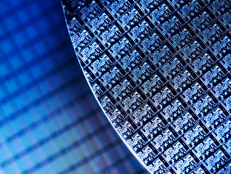
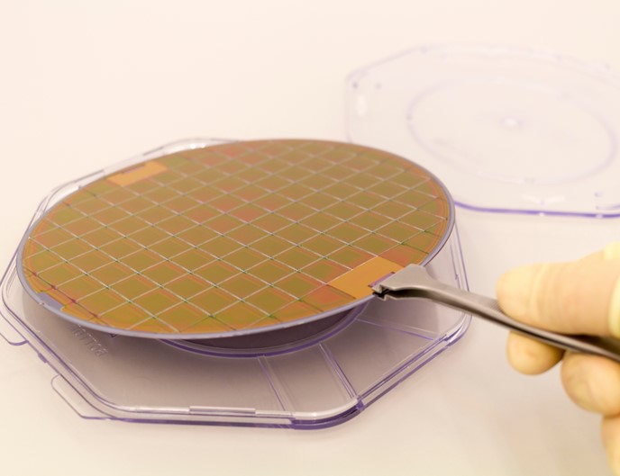
We can pattern wafer sizes ranging from 3” to 12”. Various resist coatings can be exposed e.g. AR, IP, and FujiFilms. Our current wafer materials’ exposure experience includes Glass and Silicon Wafers, but other substrates may be considered.
This technique is ideal for applications including: Microfluidics, Micro-Electro-Mechanical Systems (MEMS), BioMEMS, Micro Optics and Comparative Genomic Hybridization (CGH); Multi Project Wafers and Machine Vision Calibration Wafers.
Benefits include: the ability to reduce the prototyping cycle time, lowering the cost of small volume runs, and providing a more flexible manufacturing approach for your customer base.
- Ability to pattern feature sizes down to 1µm
- Removes mask cycle & associated costs
- Exposure area – 12”
- Various Wafers Materials considered
- Preferred resist thickness of 2µm or less
Direct Write Opportunities
- Used in production of various areas of MEMS/NEMS – for Semiconductors, Flat Panel Displays, Photonics, 2D Materials, IOT, and many other related applications.
- State-of-the-art, fast, highly precise, and exceptionally versatile technology is ideal for the use in Research & Development or prototyping, advanced packaging, Microfluidics.
- Direct-write laser system has interchangeable write heads that can pattern images ranging from 5µm or greater down to 1µm resolution.