Specialized Electronics Solutions for Fine Line Challenges
As electronics grow increasingly complex with higher functionality, clock speeds, and more diverse application requirements, our metallization solutions are developed alongside the technology to create finer lines and spaces. Constantly adapting to the needs of leading-edge electronics manufacturing customers results in our capability to deliver highly tuned processing for everything, from HDI, substrate-like PCBs, and even the most advanced IC substrates.
We continuously develop solutions for fine line resolution for the next generation of electronic devices so that our customers can meet the needs of tomorrow’s technology landscape.
IC Substrate Technologies
At the absolute leading edge of printed circuit board technologies lay the extremely dense package substrates that are used to distribute signals from Flip Chip Ball Grid Arrays (FCBGAs), Flip-Chip CSPs (FCCSPs), Wire Bond Ball Grid Arrays (BGAs), and System-in-Packages (SiPs). Our experience in the wafer level packaging markets as well as our position in the industry for decades enables us to develop a complete portfolio of solutions for the extremely fine lines and spaces required by these devices. Our solutions include a complete semi-additive process for primary metallization, panel-side copper pillar metallization, embedded trace substrate plating, 2-in-1 RDL plating, and more.
To learn more about IC substrates, click here.
modified Semi-Additive Processing
The modified Semi-Additive Process (mSAP) is a fine-line-enabling technology that was recently adapted to create the substrate-like PCBs used in today’s highest technology smartphones. Our advanced electronics manufacturing solutions for mSAP solve key issues with the technology that enable customers to increase yields, produce higher quality circuits, and tighten traces to some of the finest lines possible when starting with copper foil substrates.
To learn more about our product selection for mSAP, click here.
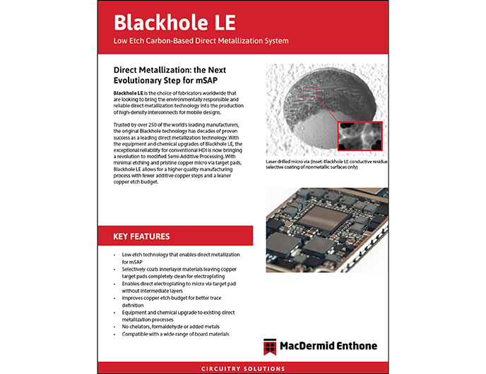
Low-Etch Direct Metallization
Our globally recognized leading carbon- and graphite-based direct metallization technologies serve as an environmentally friendly alternative to electroless coppers. Our recently upgraded low-etch technologies enable improved copper etch budgets in the manufacturing process, allowing for lower total surface plating and better trace definition after final etch.
To learn more about our direct metallization technologies, click here.
Copper Microvia Filling
MacDermid Alpha offers high performance copper microvia filling solutions and is the leading enabler of fine line designs. Keeping pace with the growth of technologies in high-density interconnects results in the development of a portfolio of via filling processes that suits any kind of board type and via dimension. From our AVF series processes that excel in extremely hard-to-fill via sizes for HDI, to our VF-TH series processes that plate copper through holes and fill microvias in a single step, customers count on our technological prowess to ensure copper filled microvias possess excellent physical properties and minimal surface copper plating.
To learn more about our via filling processes, click here.